
RF & Microwave PCB Design
RF board design from requirements through measured bring-up — 18-layer RF/mixed-signal stackups, embedded control, and verified performance.
RF boards are different
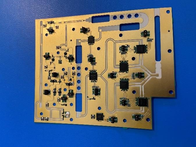
At RF and microwave frequencies the board itself is a circuit element. Stackup, controlled impedance, connector launches, grounding, and isolation are design decisions that determine whether the first prototype meets its numbers or becomes a respin. Emtera designs RF and microwave PCBs the way they have to be designed: simulate first, lay out deliberately, verify by measurement.
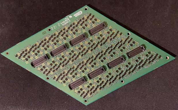
Our practice runs to 18-layer RF/mixed-signal stackups, thin array boards, and boards with integrated waveguide features, designed in ANSYS HFSS, Keysight ADS, CST, and Altium. Embedded control is part of the same discipline — ARM microcontrollers and chip-scale FPGAs integrated directly into RF boards, not bolted on as an afterthought.
Two habits keep first-pass success rates high. We place proprietary test structures on every build to independently characterize the actual board materials — measured dielectric constant and insertion loss rather than vendor datasheet values. And our simulation models are calibrated against a library of measured hardware accumulated across every prior project.
How an engagement runs
Five phases, each with defined deliverables and a go/no-go gate — so you always know where the program stands and what you’ve received.
Requirements & Feasibility
Requirements capture, architecture trade studies, risk assessment, level and link budgets.
You receive: Requirements document, feasibility assessment, program plan.
Architecture & Schematic
System architecture, component selection, schematic design, and simulation of the critical RF paths.
You receive: Schematics, bill of materials, simulation results.
Layout & Prototype
RF-aware board layout — stackup, controlled impedance, isolation, launches — with full-wave electromagnetic simulation of critical structures before fabrication.
You receive: Layout and fabrication package, assembled prototypes.
Bring-Up, Test & Verification
Prototype bring-up, debug, and measured verification against the requirement.
You receive: Test report — measured performance against specification.
Design Transfer / Production
Design-for-manufacture cleanup, documentation, and transfer to your manufacturer — or delivery of built, tested boards.
You receive: Production package — fabrication and assembly files, test procedures, documentation.
Have a project or a question?
Tell us what you're building — an engineer will get back to you.
Email contact@emtera.com