
Custom RF Semiconductors
Custom GaAs, InP, and Si designs — power amplifiers, LNAs, phase shifters, and switches — with foundry relationships and full wafer characterization.
The semiconductor floor of the stack
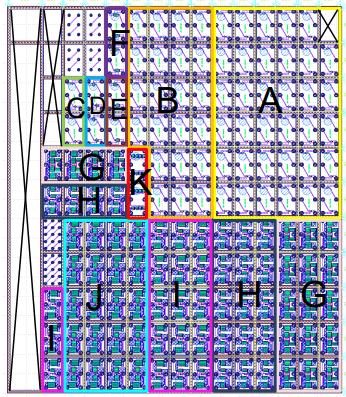
Very few RF engineering firms design their own semiconductors. Emtera does: custom GaAs, InP, and silicon devices — power amplifiers, low-noise amplifiers, phase shifters, and switches, at pitches down to 0.35 mm — through established foundry relationships, with every wafer run fully characterized and inventoried.
This is what makes the rest of the stack fast. Pretested devices with transition frequencies above 130 GHz and frequency-agnostic footprints drop directly into our rapid-development modules, and GaAs, GaN, and SiGe can be mixed freely within a single functional block. The custom PA, LNA, and phase-shifter ICs inside our Ka-band ESA came from exactly this pipeline.
Custom when it counts, COTS when it doesn’t
Custom semiconductors are a tool, not a religion. When commercial parts meet the requirement, we use them — faster and cheaper. When the application demands performance that catalog silicon can’t reach, we design the device. The judgment to know which situation you’re in is part of the service.
From wafer to system
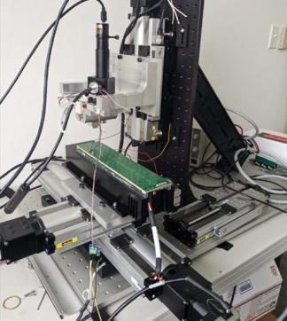
Because the same team carries a device from foundry run into modules, boards, antennas, and automated test, nothing is lost at the interfaces. Full-stack integration — semiconductor to PCB to antenna to embedded control to test to production — is extremely rare in firms of any size. It is the foundation of everything else we build.
Have a project or a question?
Tell us what you're building — an engineer will get back to you.
Email contact@emtera.com